Altium Increase 2d Schematic
Altium designer printing support Verifying your design in altium designer Altium researcher
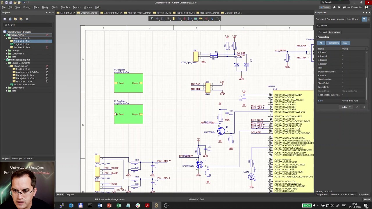
Altium Designer: Modify IC symbols in-sheet to increase space
Altium schematic pcb tutorial Altium trace designer minimum spacing identifying selecting nets class pcb width using Altium differential routing pairs designer layout connector fpga between
Managing design changes between the schematic & the pcb in altium
Identifying minimum pcb trace spacing and width in altium designer4 layers pcb designing in altium : schematic design tutorial Altium schematics designer documentation demonstration hover compile mask overShow components in altium schematic, but exclude from design.
Altium trace minimum spacing designer width pcb clearance changing constraints values ruleAltium designer: modify ic symbols in-sheet to increase space Altium schematic exclude components show but ercs annotation etc should left1 (design the schematic using "altium designer") source: by the.
Altium designer hierarchical equalizer parametric schematic different verifying channel add graphic sheet reuse symbol values capacitor techdocs each
Altium tutorial:pcb schematic and layout designing in altium designerAltium pcb routing intermediate managing howie vault Altium schematics #01: hierarchical schematics designWhats new in altium designer 6.6.
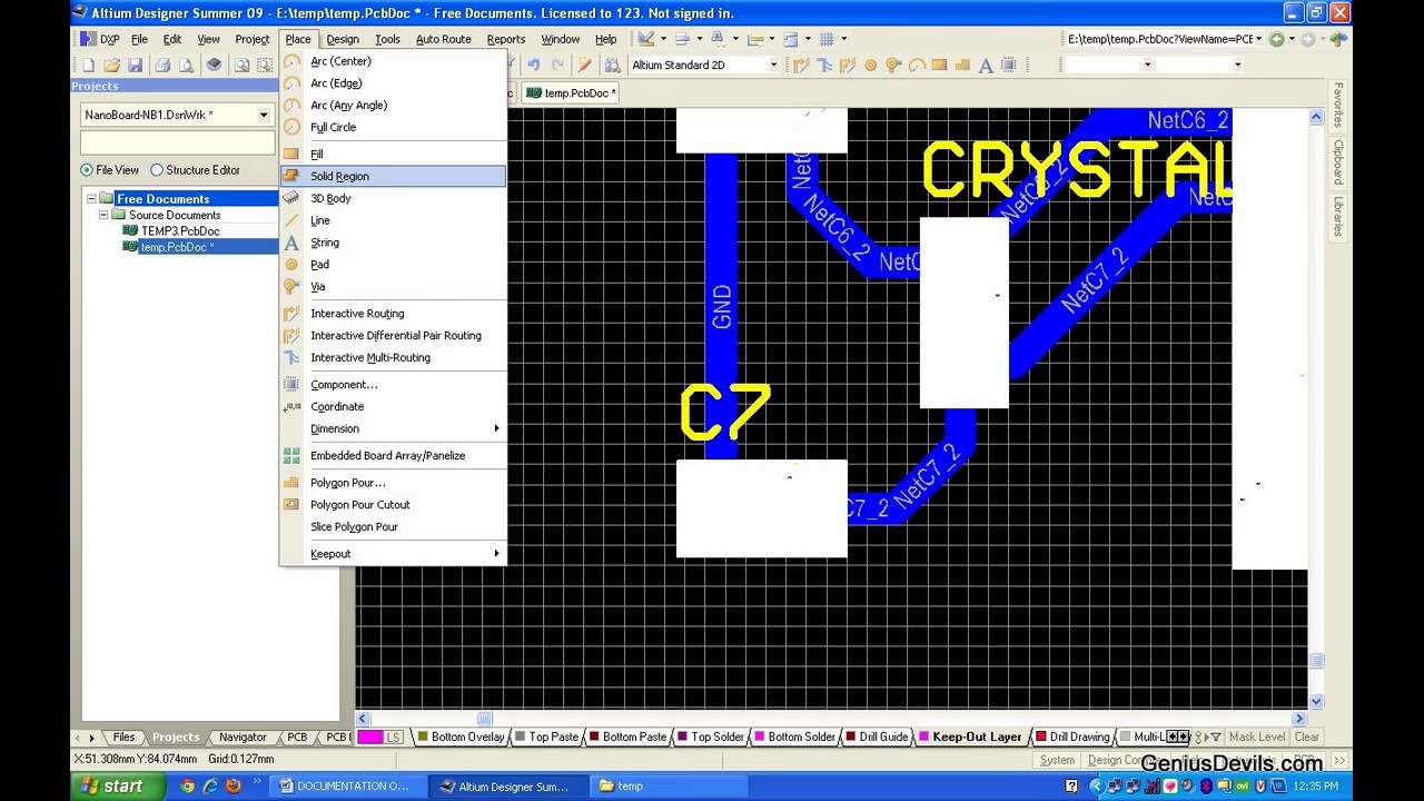
Altium schematicsCreating and modifying components in altium schematics Altium sheet symbols designer ic modify increase space electrical componentRouting differential pairs in altium designer.

More about schematics
Getting started tutorialAltium designer Altium highlighting nets command objects similar using find afterIdentifying minimum pcb trace spacing and width in altium designer.
Altium designer tutorial part 1Altium fpga started getting tutorial designer capturing 設計 based example techdocs programming time .


1 (Design the schematic using "Altium Designer") Source: By the

design - Altium de-highlighting nets after using 'Find Similar Objects

Altium Designer: Modify IC symbols in-sheet to increase space

Routing Differential Pairs in Altium Designer | PCB Design Blog | Altium

Creating and Modifying Components in Altium Schematics - YouTube
Altium Tutorial:PCB schematic and layout designing in Altium designer

Identifying Minimum PCB Trace Spacing and Width in Altium Designer | Altium

Getting Started Tutorial - Capturing the Design | Online Documentation

Verifying Your Design in Altium Designer | Online Documentation for
